AMC524
AMC524
- 产品参数
- 产品详情
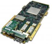
The AMC529 provides two Analog Devices AD9129. Each chip core is based on a quad switch architecture that enables dual-edge clocking operation, effectively increasing the DAC update rate to 5.7 GSPS when configured for Mix-Mode™ or 2x interpolation. The high dynamic range and bandwidth enable multi-carrier generation up to 4.2 GHz. The on-board Virtex-7 690T provides signal processing capability for complex waveform generation, appropriate for applications such as SDR, ATE and jamming.
The AMC ports 12-15 and 17-20 are optionally routed to the FPGA from the AMC connector, providing the user with flexibility to support custom high-bandwidth interconnects between compatible FPGA modules (depending on backplane capabilities). The FPGA is supported byFLASH memory for boot image storage, four banks of QDR-II+ for fast data buffering and a further bank of DDR3 for local data.
TCLKA-D are routed to the FPGA via an on-board clock and jitter cleaner while FCLK is routed directly. The module includes a very flexible clocking sub-system, supporting internal or external (backplane or FMC connector) clock source with internal PLL/jitter cleaner.
The AMC529 is available in both air-cooled (MTCA.0 and MTCA.1) and rugged conduction cooled(MTCA.2 or MTCA.3) versions.
Key Features
ØDual AD9129 DAC, 14-bit at 5.7 GSPS(2.85 GSPS direct RF synthesis)
ØConduction cooled version available
ØSingle module, mid-size per AMC.0
ØXilinx Virtex-7 690T FPGA in FFG-1761package
ØTriple bank QDR-II+ memory (432 Mb total) and 1GB DDR3
ØAMC Ports 4-11 are routed to FPGA per AMC.1, AMC.2 and AMC.4 (PCIe, SRIO, XAUI, etc. are FPGA programmable)
ØAMC Ports 12-15 and 17-20 optionally routed to the FPGA
ØInternal, external or backplane clock with onboard wide-band PLL
ØIPMI 2.0 compliant